Datapath and Microoperations
Describe clocked data movement with register-transfer notation and build buses, arithmetic circuits, logic circuits, shifters, and an arithmetic logic shift unit.
Updated
Learning objectives
- Write unconditional and conditional register-transfer statements
- Explain multiplexer and three-state-buffer implementations of a common bus
- Specify memory read and write transfers precisely
- Implement arithmetic, logic, and shift microoperations
- Trace an arithmetic logic shift unit from control word to stored result
Prerequisites
- Digital Components
A digital computer is defined internally by its registers, the microoperations performed on their stored values, and the control functions that initiate those microoperations. Register-transfer language makes that behavior precise without descending immediately to individual gates.
Timing rule: the right-hand side of a register-transfer statement is evaluated from the old state during a clock interval; the destination changes at the active edge.
| Term | Meaning in this chapter |
|---|---|
| Register transfer | Copy a word from a named source to a named destination. |
| Microoperation | One elementary operation on register contents during a clock interval. |
| Control function | A Boolean condition that enables a transfer or selects a function. |
| Bus | Shared word-wide lines carrying one selected value at a time. |
| Control word | The complete group of select and load bits applied during one interval. |
Register-Transfer Language
The statement
means that the binary content of source register is copied into destination register . is unchanged; the previous content of is overwritten. The notation assumes a path from to and a parallel-load input on .
Register names may be annotated:
- denotes a register by its function;
- denotes a selected part;
- and may denote low and high portions;
- a comma separates microoperations that occur concurrently, as in .
Two transfers separated by a comma are legal in one interval only if the datapath has the required independent sources, destinations, and write ports.
Conditional transfer
means “if control function , load from at the next active edge.” It is equivalent to the Boolean control statement
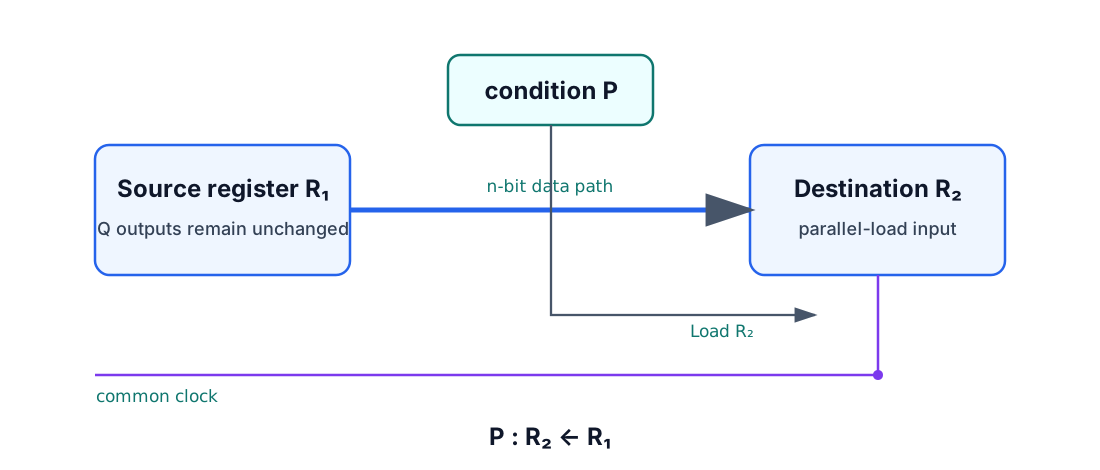
The source output can change combinationally before the edge without changing . Setup and hold constraints require the selected value and load enable to remain stable around that edge.
Common Bus Systems
Dedicated wires between every pair of registers scale poorly. A common bus lets many registers share one set of word-wide lines.
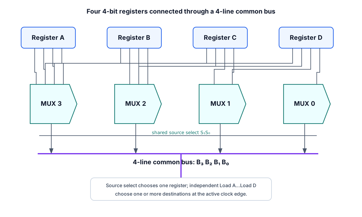
For registers , source select may use:
| Bus source | |
|---|---|
| 00 | |
| 01 | |
| 10 | |
| 11 |
To perform , the controller selects onto the bus and asserts LoadR2:
The two symbolic actions describe one physical transfer: source selection is combinational; destination loading is clocked.
Bus hardware grows with both register count and word width. Eight 16-bit source registers require sixteen 8-to-1 multiplexers—one for each bus bit—and shared source-select bits. Destination selection is separate: a 3-to-8 decoder can produce eight one-hot load enables. This separation is why several destinations may capture one selected source, while two different sources cannot occupy a single bus simultaneously.
Three-state bus
A multiplexer bus may be replaced by one three-state buffer per source bit. A buffer output can be 0, 1, or high impedance . Exactly one register’s buffers may be enabled at a time:
- no enabled source leaves the bus floating unless pull or hold circuitry is provided;
- two enabled sources can contend, producing an invalid level and excessive current;
- decoder-generated one-hot enables prevent contention.
Memory Transfers
denotes the memory word whose address is held in address register .
| Operation | Register-transfer statement | Required control |
|---|---|---|
| Read | Address valid, memory read asserted, destination load after data is valid | |
| Write | Address and data valid while memory write is asserted |
A read does not destroy the memory word. A write changes memory state and therefore must not be asserted until address and data are stable.
Four Classes of Microoperations
- Register transfer: copy binary information.
- Arithmetic: interpret words as numbers and add, subtract, increment, or decrement.
- Logic: manipulate corresponding bits without numeric carry.
- Shift: move bit positions logically, arithmetically, or circularly.
The classes describe meaning. One physical ALU may implement several classes by changing its select inputs.
Arithmetic Microoperations
Parallel adder
An -bit ripple-carry adder chains full adders:
must propagate to the next stage. This makes ripple delay grow with word width.
Adder-subtractor
A common circuit uses mode to complement every input and supply the initial carry:
| Operation | |||
|---|---|---|---|
| 0 | 0 | ||
| 1 | 1 |
For unsigned subtraction, final carry 1 means no borrow. For two’s-complement signed arithmetic, carry out is not the overflow test:
For example, with four bits, gives 0111 + 0011 = 1010. The carry into the sign bit is 1 and the carry out is 0, so : two positive operands produced a negative four-bit pattern.
Increment and decrement
Increment is . A chain of half adders can propagate the initial 1, or an existing adder can use a zero second operand and . Decrement may add an all-ones word:
Multifunction arithmetic circuit
If multiplexers choose , one parallel adder computes :
| Result | |||
|---|---|---|---|
| 00 | 0 | Transfer | |
| 00 | 1 | Increment | |
| 01 | 0 | ||
| 01 | 1 | ||
| 10 | 0 | ||
| 10 | 1 | ||
| 11 | 0 | all ones | Decrement |
| 11 | 1 | all ones | Transfer with carry out |
Logic Microoperations
Logic operations act independently on bit pairs. If and :
| Operation | Bitwise result |
|---|---|
1000 | |
1110 | |
0110 | |
0011 |
AND can clear selected bits, OR can set selected bits, XOR can toggle selected bits, and a mask can isolate a field. All 16 Boolean functions of two variables are possible, but an ALU commonly implements a useful subset.
Shift Microoperations
| Shift | Inserted bit | Primary interpretation |
|---|---|---|
| Logical left/right | 0 | Unsigned multiply/divide by two when no significant bit is lost |
| Arithmetic right | Old sign bit | Signed two’s-complement division by two with rounding caveats |
| Circular left/right | Bit shifted out at opposite end | Rotation, field manipulation, some cryptographic operations |
For 10110110:
- logical right →
01011011; - arithmetic right →
11011011; - rotate right →
01011011because the old low bit happened to be0.
Arithmetic Logic Shift Unit
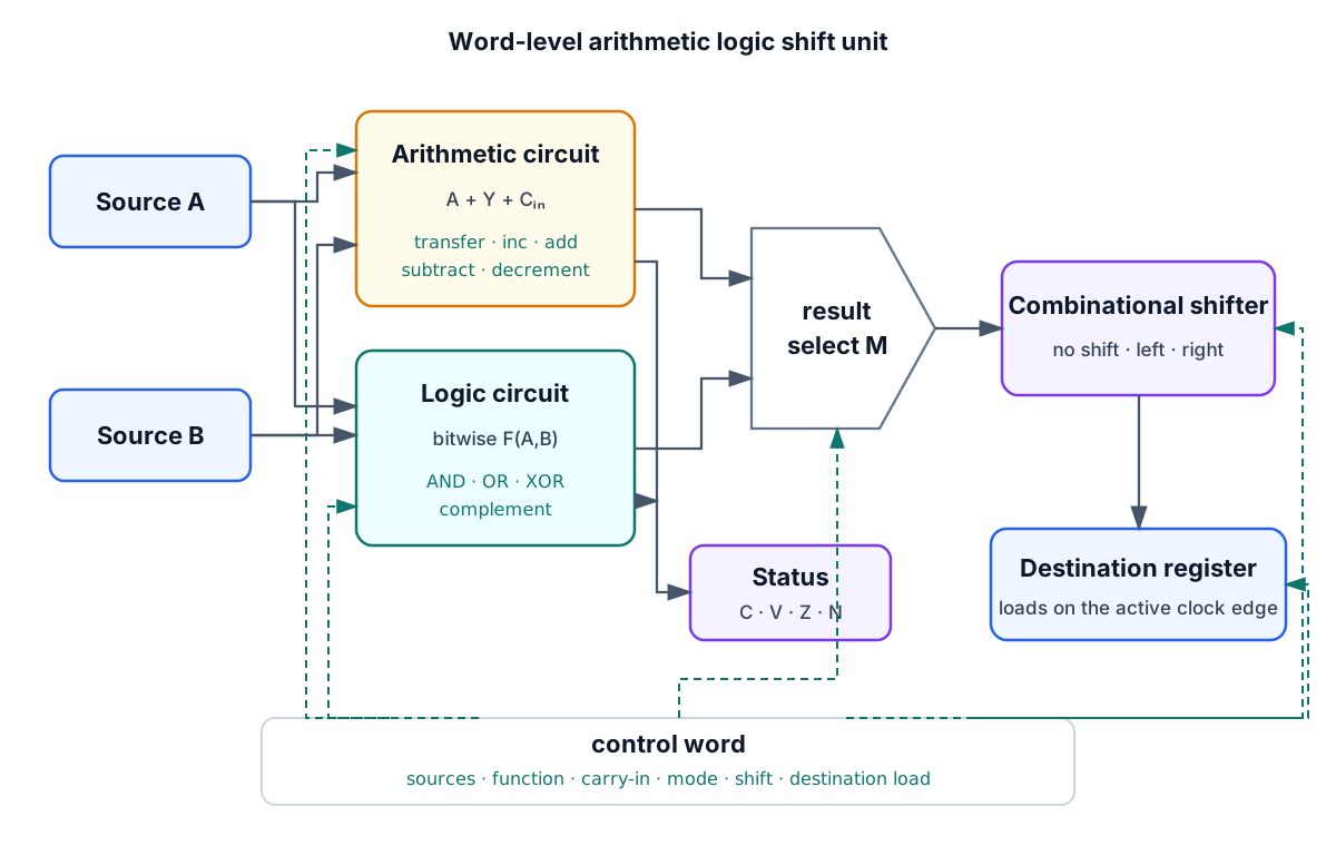
A typical control word contains:
| Field | Purpose |
|---|---|
| Source A / source B | Select operand registers |
| Mode | Choose arithmetic or logic unit |
| Function | Choose add, subtract, AND, OR, XOR, complement, and so on |
| Carry in | Complete increment or two’s-complement subtraction |
| Shift | No shift, left, or right |
| Destination | Select register load enable |
Suppose , , the arithmetic function is add, carry in is 0, and shift is logical right. The combinational stages produce:
The destination remains unchanged during the interval and becomes 0100 only on the active edge.
Timing one microoperation
For , the active path may be source register operand multiplexers ALU destination register. Suppose the delays are:
| Component | Delay |
|---|---|
| Source clock-to-Q | 80 ps |
| Operand selection | 140 ps |
| Addition | 350 ps |
| Destination setup | 70 ps |
Ignoring skew, the clock period must be at least
so this datapath cannot exceed about GHz. A logic AND using a 90 ps ALU path finishes sooner, but a common clock must still accommodate the slower addition. Pipelining can divide the long path, at the cost of extra registers, latency, and control complexity.
Datapath Resource Conflicts
With one common bus, only one source can drive it during an interval. The simultaneous transfers
cannot both occur if they require different bus sources. The controller must use two cycles or the datapath must provide a second read path. Register-transfer notation is therefore also a resource specification.
Self-Check
- Which part of is combinational and which part is clocked?
- Why are and signed overflow different?
- For and , compute with four-bit two’s-complement addition.
- Can two destination registers load the same bus value on one edge?
- How many bit-slice multiplexers and select bits are required to place one of 16 different 32-bit registers on a common bus?
Answers
- Evaluating and routing are combinational; storing into is clocked.
- Carry describes the unsigned boundary; signed overflow compares the carries into and out of the sign position.
- , so the four-bit result is
0110. - Yes, if both load enables are asserted and electrical fan-out permits it.
- Thirty-two 16-to-1 multiplexers and four shared select bits.