Control Unit Design
Design hardwired CPU control as a finite-state machine: specify the datapath, derive microoperations and control signals, and implement one-hot, encoded, PLA, or ROM controllers.
Updated
Learning objectives
- Separate a digital system into its datapath and control unit
- Translate an algorithmic flowchart into a control-state diagram and timed microoperations
- Derive control words, next-state equations, and flip-flop excitation equations
- Trace hardwired controllers for signed addition/subtraction and shift-and-add multiplication
- Compare one-hot, encoded, PLA, and ROM control implementations
Prerequisites
- Datapath and Microoperations
- Computer Arithmetic
A processor datapath can add, complement, shift, load, and clear values, but it does not decide when those operations happen. The control unit supplies that sequence. It observes an operation request and datapath status, enters a state, asserts the corresponding control signals, and moves to the next state on a clock edge.
This chapter develops that idea through two complete hardwired-control examples. The first uses one flip-flop per state to control sign-magnitude addition and subtraction. The second encodes four multiplication states in two flip-flops. The examples expose the same reusable design path:
algorithm -> datapath -> state diagram -> control table -> Boolean logicCentral idea: the datapath performs microoperations; the controller sequences them. A correct arithmetic algorithm is not yet a hardware design until every operation has a destination register, a control signal, a state, and a clock edge.
Control-Unit Foundations
| Term | Controller meaning |
|---|---|
| State | The controller’s stored memory of which step is currently active. |
| Status input | A datapath condition, such as zero, sign, carry, or a tested multiplier bit. |
| Control signal | One bit that selects a route, ALU function, register load, shift, or clear. |
| Control word | All control signals asserted together during one state. |
| Next-state logic | Combinational logic that chooses the state loaded at the next clock edge. |
Datapath and controller
The two parts form a synchronous feedback loop. The controller says what to do now; the datapath reports what just happened.
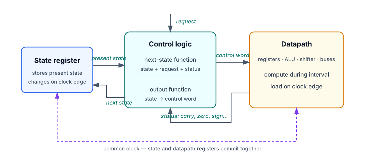
The visual key is consistent throughout the chapter: blue identifies stored state and registers, teal identifies control and decisions, amber identifies arithmetic or datapath actions, and purple identifies status, correction, and shift operations. The colours explain hardware roles; the connections and branches retain the structure of the source figures.
| Part | Contains | Receives | Produces |
|---|---|---|---|
| Datapath | Registers, ALU, shifter, buses, status flip-flops | Operand data and control signals | Results and status conditions |
| Controller | State register and next-state/output logic | Requests, status conditions, and clock | ALU selects, register enables, and completion signals |
A microoperation is an elementary register action completed in one clock interval, such as , , or . Register-transfer notation names the destination on the left and the value computed during that interval on the right.
Suppose and . While the controller is in an “add” state, it selects the ALU’s add function and asserts the load enable for . The ALU output changes combinationally to 1000, but the stored value of remains 0101 until the active clock edge. At that edge, becomes 1000 and the controller enters its next state.
during the interval: current state -> control signals -> ALU result
at the clock edge:   registers load result; state register loads next state
after the edge:      new state and new register values are visible
This “compute during the interval, commit at the edge” model explains why a status value written by one state is normally tested by the following state.
From an algorithm to hardware
- Write the algorithm. Show operations, decisions, repetition, and termination.
- Specify the datapath. Choose registers and functional units, then name every control input and status output.
- Assign control states. A state groups compatible microoperations that can occur on one active clock edge.
- Draw transitions. Label every conditional edge and account for every input combination.
- Create the output table. For each state, identify the required datapath control word.
- Choose an encoding. Use one-hot, binary, Gray, or another justified assignment.
- Derive and verify logic. Obtain next-state and output equations, then trace normal and boundary cases.
The conversion from flowchart to state diagram is not unique. Two controllers may implement the same algorithm with different state counts. A valid choice must still respect hardware constraints: a register cannot be loaded before its source is ready, a status bit written on an edge cannot be tested before the following state, and incompatible transfers cannot share one resource in the same cycle.
Example 1: Sign-Magnitude Addition and Subtraction
Problem and notation
Two sign-magnitude operands are split into sign bits and magnitude registers . The controller accepts separate add and subtract requests.
With a four-bit magnitude, the representation has one separate sign bit:
| Value | Sign | Magnitude | Written as |
|---|---|---|---|
| 0 | 0101 | 0 0101 | |
| 1 | 0101 | 1 0101 | |
| 0 | 0000 | 0 0000 | |
| 1 | 0000 | 1 0000 |
The magnitude is ordinary unsigned binary. The sign bit is not part of a two’s-complement word. This is why the hardware must decide separately what to do with the signs and the magnitudes—and why sign-magnitude has two encodings for zero.
| Symbol | Meaning |
|---|---|
| Request addition | |
| Request subtraction | |
0 when the effective signs match; 1 when they differ | |
| ALU end carry/status flip-flop | |
| Current ALU carry output | |
| Ready/initial-state output |
Subtraction is reduced to addition by first complementing . The controller can then apply one common rule: add magnitudes when the effective signs match; otherwise subtract the smaller magnitude from the larger one.
The design assumes and are mutually exclusive request pulses. If an interface can assert both—or hold either request high after completion—the controller needs explicit priority and acknowledgement rules.
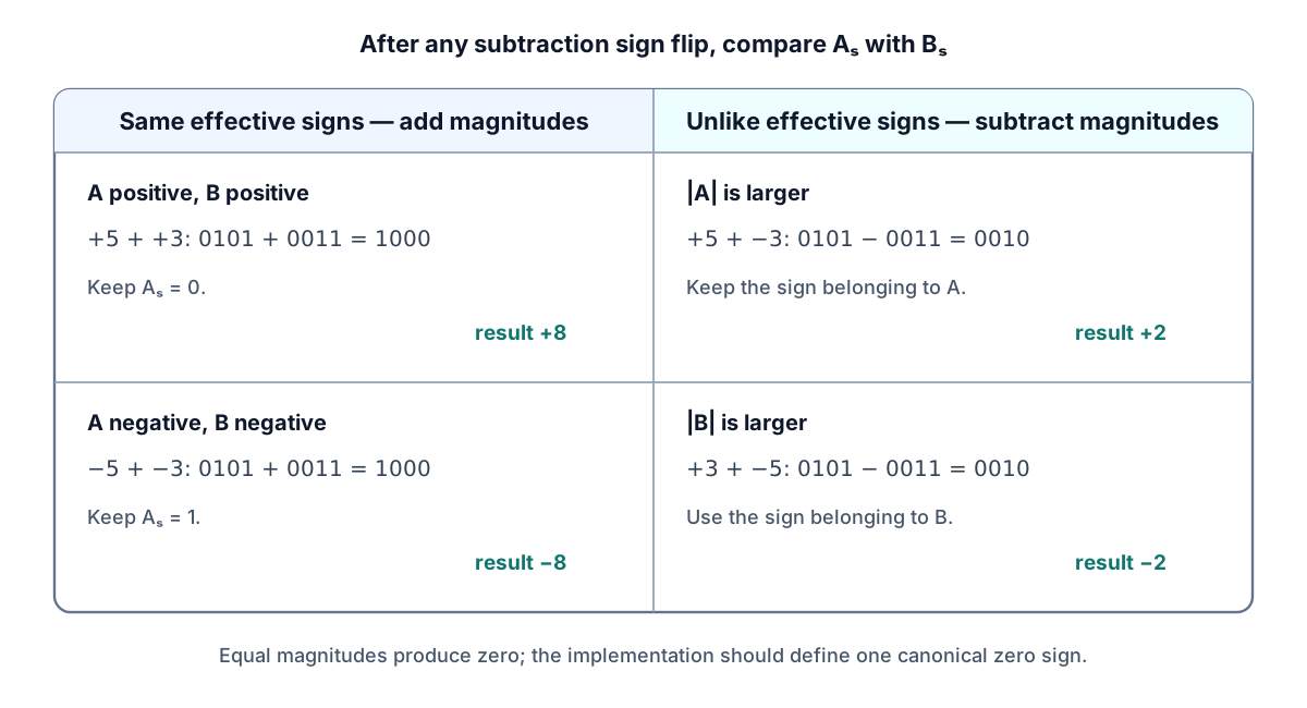
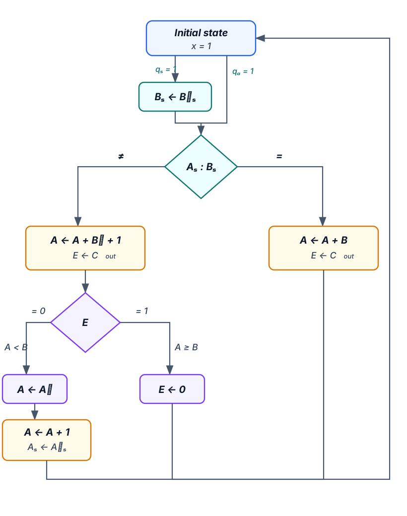
Reading the algorithm
- With equal effective signs, compute . The sign already belongs to the result, and records magnitude overflow.
- With unlike signs, compute . This is using two’s-complement addition. Ordinary signed overflow is not possible in this branch.
- If the subtraction produces an end carry, there was no borrow: the magnitude in is already non-negative. Clear and retain .
- If there is no end carry, then . The register contains a negative two’s-complement intermediate value. Complement and increment to recover its magnitude, then complement so the sign follows the operand with the larger magnitude.
The correction is split into and because the available ALU provides complement and increment, but not a single “two’s complement” function. When the magnitudes are equal, the subtraction magnitude is zero; a practical design should also define whether zero is canonicalised to a positive sign.
Numeric examples: every arithmetic path
Use four-bit magnitude registers throughout these examples:
| Operation | Effective sign relation | Magnitude calculation | Result |
|---|---|---|---|
| Same | 0101 + 0011 = 1000 | ||
| Same | 0101 + 0011 = 1000 | ||
| Unlike, | 0101 − 0011 = 0010 | ||
| Unlike, | 0101 − 0011 = 0010 |
The datapath does not contain a magnitude comparator. It discovers which magnitude is larger from the carry produced by two’s-complement subtraction.
For , , , so and the controller subtracts:
  A              0101
  complement B   1100
  input carry    0001
                 ----
                 1 0010
The stored magnitude is 0010 and . End carry 1 means no borrow, so ; the sign stays , producing .
For , the same circuit produces a negative intermediate result:
  A              0011
  complement B   1010
  input carry    0001
                 ----
                   1110   E = 0

  complement     0001
  increment      0010
  flip A_s       0 -> 1
No end carry means a borrow occurred and . States and convert 1110 to magnitude 0010 and reverse the sign, producing .
A subtraction request only changes the effective sign of . For example, first changes from 1 to 0; the controller then sees equal signs and adds the magnitudes, obtaining .
Finally, four magnitude bits can hold at most . For , 1001 + 1000 = 1 0001: receives 0001, while reports that the mathematical result did not fit. The carry must be interpreted as overflow in the equal-sign addition path, not as a fifth magnitude bit silently discarded.
Datapath specification
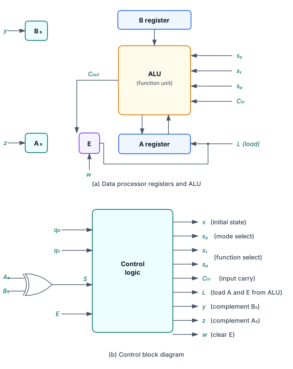
The ALU receives , , the selection word , and input carry . Signal loads the ALU result into and into . Three direct controls handle operations outside the ALU:
| Control | Datapath action |
|---|---|
| Complement | |
| Complement | |
| Clear |
The controller inputs are , , , and . Although and enter the comparison logic physically, using reduces the controller’s sign decision to one variable.
Control-state diagram
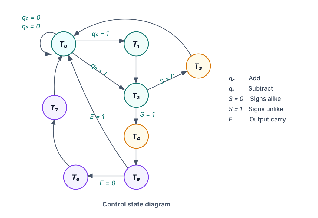
The state sequence is deliberately explicit:
- is idle and asserts . It stays there while both requests are low.
- A subtract request enters to complement ; an add request can go directly to .
- tests the updated sign relation . Matching signs select ; unlike signs select .
- adds magnitudes and finishes. subtracts magnitudes and stores the end carry.
- clears overflow status and chooses whether result correction is needed.
- and form the two’s complement of and reverse before returning to idle.
The value is written on the edge that leaves . Therefore the controller tests in , not in . Clearing while leaving is safe: the old value selects the outgoing edge during the interval, and the edge simultaneously stores the next state and clears .
Clock trace: positive 3 plus negative 5
The numeric example becomes a hardware execution when placed on clock intervals. Initial values are , , , and :
| Interval | Current state | Condition seen during interval | Transfer committed at edge | State after edge |
|---|---|---|---|---|
| 0 | None | |||
| 1 | None | |||
| 2 | Unlike signs | |||
| 3 | Stored | |||
| 4 | Correction required | |||
| 5 | Final correction |
There are six state intervals from accepting the request to becoming ready again. Only three intervals change arithmetic data: , , and . The other intervals route the controller using conditions that are stable for the entire interval.
State outputs and microoperations
| State | Microoperation | |||||||
|---|---|---|---|---|---|---|---|---|
| Initial/ready state | 1 | 000 | 0 | 0 | 0 | 0 | 0 | |
| 0 | 000 | 0 | 0 | 1 | 0 | 0 | ||
| No transfer; evaluate | 0 | 000 | 0 | 0 | 0 | 0 | 0 | |
| 0 | 001 | 0 | 1 | 0 | 0 | 0 | ||
| 0 | 010 | 1 | 1 | 0 | 0 | 0 | ||
| 0 | 000 | 0 | 0 | 0 | 0 | 1 | ||
| 0 | 111 | 0 | 1 | 0 | 0 | 0 | ||
| 0 | 000 | 1 | 1 | 0 | 1 | 0 |
The load signal must be 1 whenever an ALU result is intended to change (and, where relevant, ). In other states, the ALU may still produce a combinational value, but it has no architectural effect.
One-hot implementation
Assign one D flip-flop to each state and use the flip-flop output itself as the timing variable . Exactly one state bit is high. To obtain a D-input equation, AND each incoming transition condition with its source state and OR all paths entering the destination:
Read each equation as an answer to “when must this state become 1?” For example:
- is entered from when , or from unconditionally. Therefore .
- is entered only from when . Therefore .
- has four incoming paths: its idle self-loop, completion from , the branch from , and completion from . OR-ing those products gives .
Output equations are even more direct: OR the states whose table row contains 1 for that signal.
As a quick check, let the current state be . Then only , so , , and . Those are exactly the controls required for . In , none of the ALU or load equations is asserted; that state exists only to choose the next path.
One-hot control uses eight flip-flops here, but the logic is regular and can be read directly from the state diagram. A compact binary assignment would use only three flip-flops, at the cost of decoding states and usually more intricate next-state logic.
Example 2: Shift-and-Add Binary Multiplication
Datapath algorithm
Let hold the multiplicand, hold the multiplier, accumulate the partial product, hold the adder carry, and count the remaining bit positions. The final -bit magnitude appears in the concatenated registers . The result sign is .
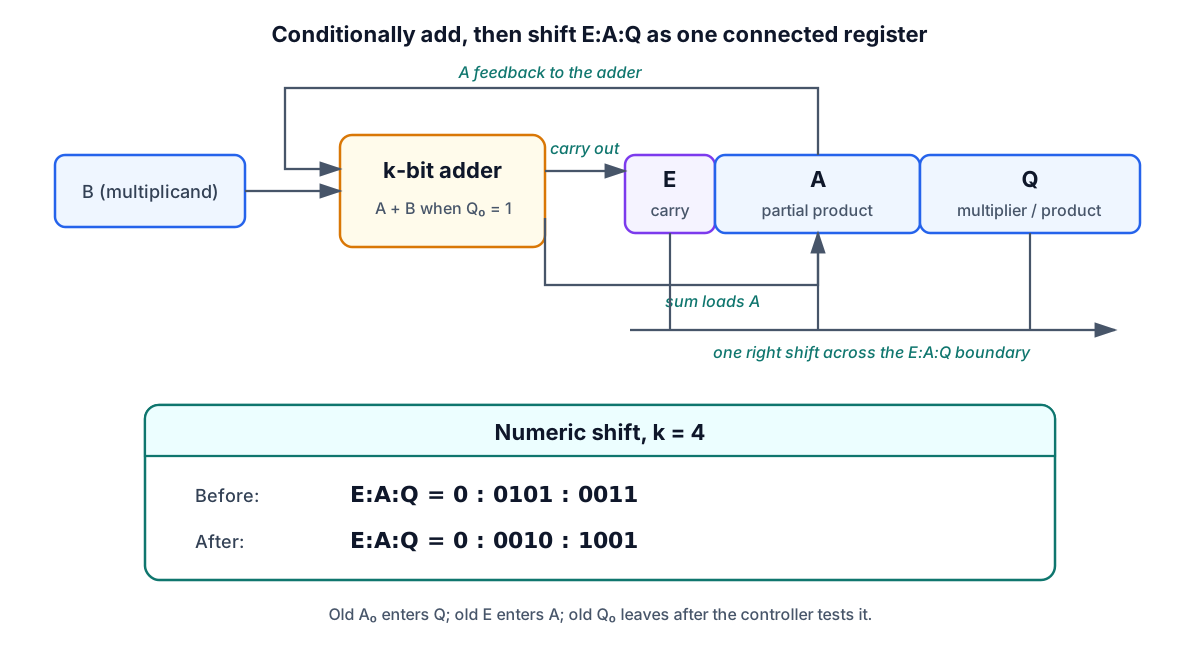
For , the shift register is nine bits wide: one carry bit, four accumulator bits, and four multiplier bits. If EAQ = 0 0101 0011, one right shift produces 0 0010 1001. The old least-significant bit of becomes the new most-significant bit of ; the old becomes the new most-significant bit of . This is why must participate in the shift rather than being discarded after an addition.
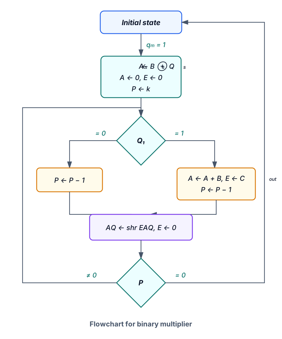
On a multiply request :
- Initialise , , , and set the product sign.
- Inspect , the current least-significant multiplier bit. If it is
1, perform and . - Always perform .
- Shift the concatenated value: , then clear .
- If , repeat from the bit test; otherwise return to idle.
Each shift places one newly settled product bit into and exposes the next multiplier bit at . After iterations, contains the most-significant half and the least-significant half. denotes the zero test: exactly when .
The useful invariant is: before iteration , the unprocessed multiplier bits remain in , while the partial product accumulated so far occupies the left side of . Testing decides whether the current power-of-two copy of contributes to the product; the shift then aligns the registers for the next bit.
Four-state controller
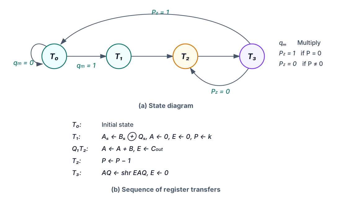
| State | Register transfers |
|---|---|
| Initial state; wait for | |
| If : ; always | |
| ; test |
The conditional control function for loading the sum is . In contrast, the decrement is enabled by alone. Moving the decrement into makes the new counter value available for the decision in .
Worked trace: multiplying 5 by 3
For , begin with , , , and :
| Iteration | EAQ before add | E after optional add | A after shift | after decrement | |
|---|---|---|---|---|---|
| 1 | 0 0000 0011 | 1 | 0:0101 | 0010:1001 | 3 |
| 2 | 0 0010 1001 | 1 | 0:0111 | 0011:1100 | 2 |
| 3 | 0 0011 1100 | 0 | 0:0011 (unchanged) | 0001:1110 | 1 |
| 4 | 0 0001 1110 | 0 | 0:0001 (unchanged) | 0000:1111 | 0 |
Look closely at iteration 1. Because , the datapath first adds 0000 + 0101, making E:A = 0:0101. It then shifts the complete string 0 0101 0011 to 0 0010 1001. Reversing those two actions would produce a different—and incorrect—partial product.
The final concatenation is . If the original operands were and , the magnitude trace would be identical; only would change, so the interpreted result would be .
The carry register matters when an addition exceeds four bits. If and , their sum is 1 0110. Storing E:A = 1:0110 and then shifting preserves the leading 1 as the new most-significant bit of .
Encoded-state excitation table
Encode as in state bits . For JK flip-flops, X is a don’t-care excitation:
| Present bit | Required next bit | Required excitation |
|---|---|---|
| 0 | 0 | , |
| 0 | 1 | , |
| 1 | 0 | , |
| 1 | 1 | , |
Apply these four rules independently to and in every state-table row.
| Present | Next | ||||||||
|---|---|---|---|---|---|---|---|---|---|
| 00 | 0 | X | 00 | 0 | X | 0 | X | ||
| 00 | 1 | X | 01 | 0 | X | 1 | X | ||
| 01 | X | X | 10 | 1 | X | X | 1 | ||
| 10 | X | X | 11 | X | 0 | 1 | X | ||
| 11 | X | 0 | 10 | X | 0 | X | 1 | ||
| 11 | X | 1 | 00 | X | 1 | X | 1 |
Inspection and simplification give:
Here is how to read the result:
- must change from
0to1only when leaving , so . - must reset while leaving only when the counter is zero, so .
- must set for the request transition and for , so .
- Whenever —in or —the next state’s is
0. Choosing therefore handles both cases; its value is irrelevant while .
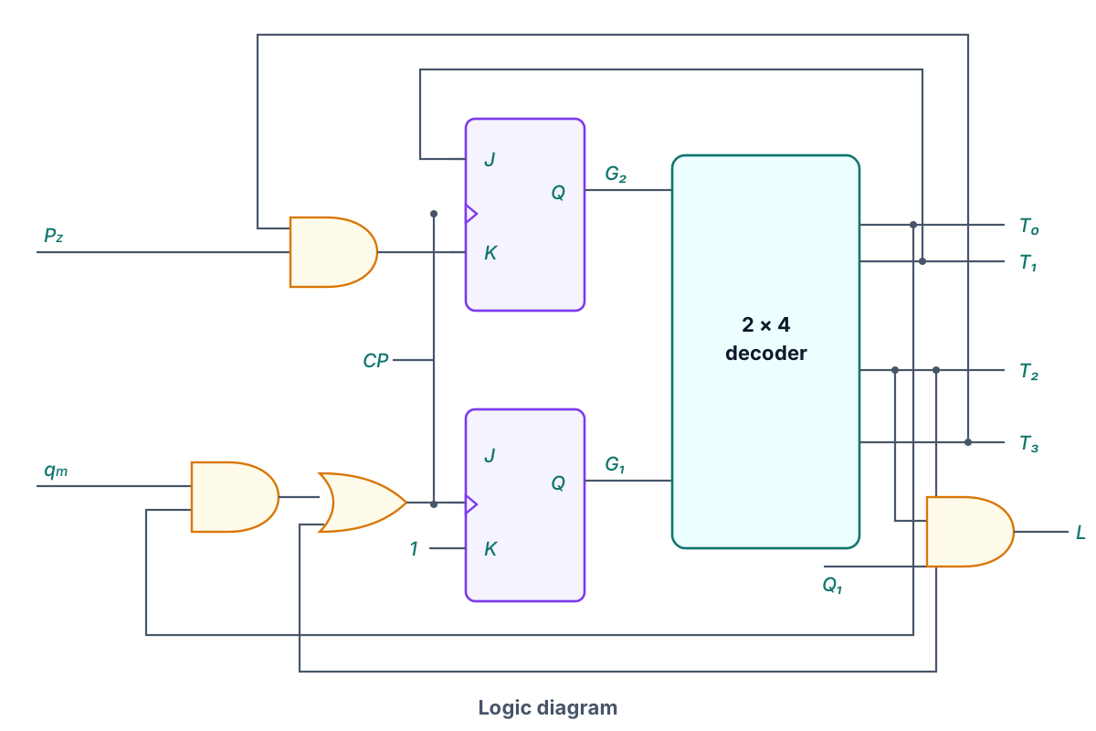
Equations derived by inspection are candidates, not proof. Substitute every table row—or simulate all reachable state/input combinations—to confirm that the resulting circuit produces the specified transitions. This four-state example uses every two-bit encoding; a controller with unused encodings should also define a safe recovery path, usually to the idle state.
PLA and ROM Control
A hardwired controller combines a state register with fixed gates and decoders. The combinational part can instead be replaced by a programmable logic array (PLA). The state register still holds the current control state; the PLA receives that state plus external/status inputs and produces both the next-state bits and datapath control outputs.
The state table already contains the information needed to create a PLA program table or a ROM truth table:
address/input side: current state + requests + status
data/output side: next state + datapath controls| Implementation | State storage | Combinational implementation | Best fit | Main trade-off |
|---|---|---|---|---|
| One-hot hardwired | One flip-flop per state | Small AND/OR equations | Few states, clarity, fast decoding | More flip-flops |
| Encoded hardwired | state bits | Custom next-state and decode logic | Regular small controllers | Equations can become irregular |
| PLA control | Encoded state register | Programmable product and sum terms | Tables with many useful don’t-cares | Requires careful minimisation and verification |
| ROM control | Encoded state register or address field | Stored truth table | Dense or highly irregular tables | May store many redundant combinations |
A PLA is attractive when shared product terms and don’t-care entries reduce the logic. A ROM is often simpler when most combinations need explicit outputs. In both cases, “programmable” refers to the combinational mapping; the clocked state register still determines the control sequence.
For a concrete sizing comparison, the multiplier has two state bits and two relevant inputs, and . A ROM indexed by all four bits needs words. If the controller needs two next-state bits and six datapath controls, each word is eight bits, for a total of stored bits—even though several address combinations behave identically. A PLA can express only the required product terms, such as , , and , and share them between outputs. The ROM is more regular; the PLA may be smaller when the table is sparse.
A Controlled Accumulator Bit Slice
A compact accumulator unit shows how a control word becomes gates. Nine mutually exclusive variables select one register operation:
| Control | Register transfer | Function | Control | Register transfer | Function |
|---|---|---|---|---|---|
| Add | Exclusive OR | ||||
| Clear | Shift right | ||||
| Complement | Shift left | ||||
| AND | Increment | ||||
| OR |
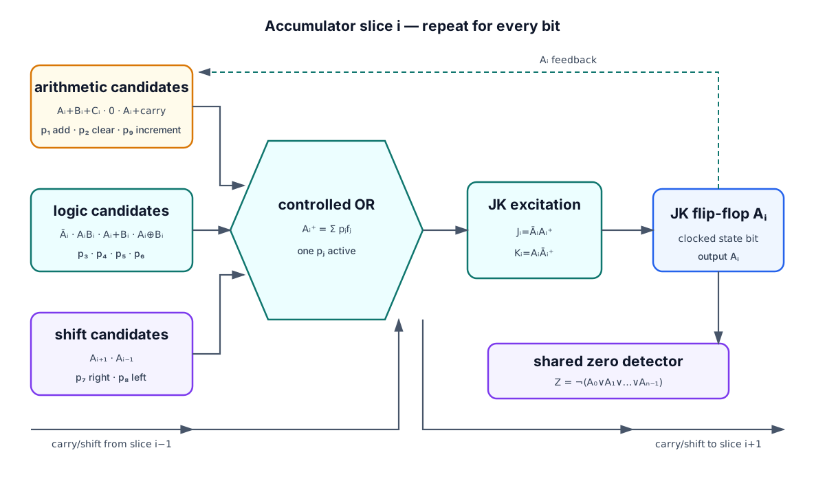
For each bit , combinational logic forms the requested next value . A D flip-flop could load that value directly. With a JK flip-flop, the excitation can be written and . Because the controls are mutually exclusive, their candidate next values can be ORed without two operations fighting for the same destination.
The add and increment terms propagate carry from bit to ; shift-right takes , shift-left takes , with defined serial inputs at the ends. A zero-status output is
This slice is the gate-level version of a control table: each symbolic transfer must have a data path, and each must activate exactly that path at the clock edge.
From Arithmetic Control to CPU Control
An instruction controller uses exactly the same construction at a larger scale. Its datapath adds a program counter, instruction register, memory interface, register file, and condition flags. A simple multicycle fetch might be divided as follows:
| State | Representative microoperations | Why it needs a state |
|---|---|---|
| Fetch address | Present a stable memory address | |
| Fetch data | Wait for/read memory and advance the program counter | |
| Capture and decode | ; decode opcode | Store the instruction before selecting an execution path |
| Execute | Instruction-specific ALU, memory, or branch transfers | Different opcodes activate different datapath resources |
| Write back | Destination register result | Commit the architectural result |
An opcode plays the role of an operation request; zero, carry, overflow, and comparison flags play the role of , , , and ; and the controller outputs become mux selects, ALU functions, memory enables, and register write enables. Pipelining later overlaps these phases, but it does not remove the need to generate correct control for each stage.
For example, suppose PC = 0x20 and memory location 0x20 contains ADD R3, R1, R2, with R1 = 9 and R2 = 6:
| State | Values before edge | Controls and computation | Values after edge |
|---|---|---|---|
| Fetch address | PC = 0x20 | Route PC to memory-address input; load MAR | MAR = 0x20 |
| Fetch data | M[0x20] = ADD... | Read memory; increment PC by 4 | MDR = ADD..., PC = 0x24 |
| Decode | MDR = ADD R3,R1,R2 | Load IR; select the ADD path | IR = ADD R3,R1,R2 |
| Execute | R1 = 9, R2 = 6 | Select register operands and ALU addition | ALUOut = 15 |
| Write back | ALUOut = 15 | Enable destination R3 | R3 = 15 |
The arithmetic is simple; the controller’s job is to guarantee that the correct sources, destination, ALU function, and write enable are selected in the correct intervals. A mistaken R3 write enable one interval early would store an old value even if the ALU itself were perfect.
Design Checks and Refinements
Before treating a controller as complete, check the following:
- Idle protocol: Is there a ready signal, and what happens if requests overlap or remain asserted?
- Complete transitions: Does every reachable state define a next state for every relevant condition?
- Clock semantics: Is each decision based on a value that was already stored before the active edge?
- Control safety: Are incompatible enables mutually exclusive, and are write enables low when results should be ignored?
- Arithmetic boundaries: What happens for zero, equal magnitudes, maximum carry, negative zero, and the most negative representable value?
- Counter convention: Is the loop count tested before or after decrement, and does the controller run exactly iterations?
- Reset and recovery: Which state is entered after reset, and can an illegal encoded state return safely to idle?
- Equation verification: Do the simplified equations reproduce every state-table row, including intended don’t-cares?
The two examples differ in arithmetic and encoding, but their architecture is the same: status flows from datapath to controller, control flows back to datapath, and the state register turns an algorithm into a clock-by-clock sequence. That pattern scales from a small arithmetic unit to the instruction fetch-decode-execute controller of a CPU.
Quick self-check
- Why is tested in rather than in ?
- For , which arithmetic branch runs, and what sign should the result have?
- In the multiplier, why is the shift applied to
EAQrather than onlyAQ? - Which term in keeps the sign-magnitude controller idle when no request is present?
Answers
- T₄ stores the ALU carry into E on its outgoing clock edge. T₅ is the first interval in which that stored value is stable and available for a transition decision.
- The signs differ, so the controller subtracts magnitudes. Since 6 is larger than 2, it retains A's negative sign and produces −4.
- An addition may produce a carry in E. Including E in the right shift moves that bit into the most-significant position of A instead of losing it.
- The idle self-loop term is q̅ₐq̅ₛT₀.