Digital Components
Build architectural storage and selection structures from integrated circuits, decoders, encoders, multiplexers, registers, shift registers, counters, and memory arrays.
Updated
Learning objectives
- Relate gates, integrated-circuit families, and digital modules
- Use decoders, encoders, multiplexers, and demultiplexers as selection circuits
- Explain basic, parallel-load, shift, and bidirectional registers
- Derive next-state behavior for a universal shift register and binary counter
- Determine memory capacity and required address and data lines
Prerequisites
- Computer Organization
- Boolean functions, truth tables, and flip-flops
Processor datapaths are assembled from reusable digital modules. Gates implement Boolean functions; flip-flops retain one bit; integrated circuits package many such devices; and larger modules—registers, decoders, multiplexers, counters, and memories—give architecture diagrams their familiar building blocks.
Storage versus selection: a register remembers a value across clock cycles. A decoder or multiplexer merely selects a path from current inputs. Confusing state with combinational selection is a common source of timing errors.
Vocabulary for this chapter
| Term | Precise meaning |
|---|---|
| Combinational circuit | Its output is a function of current inputs only; it has no remembered state. |
| Sequential circuit | Its next output can depend on stored state as well as current inputs. |
| Word | A fixed-width group of bits treated as one unit, such as a 16-bit register value. |
| Active clock edge | The rising or falling transition on which a storage element accepts its next value. |
| Enable | A control input that permits an operation while leaving the shared clock unchanged. |
Integrated Circuits and Logic Families
An integrated circuit (IC) is a silicon chip containing interconnected electronic devices. The chip is mounted in a package whose pins provide power, inputs, and outputs. A small package may expose roughly 14 pins; larger packages can expose hundreds or thousands.
Digital circuits were historically grouped by the devices and circuit style used to implement their gates:
| Family | Device basis | Characteristic emphasis |
|---|---|---|
| PMOS/NMOS | One MOS transistor polarity | High component density; older families had asymmetric behavior |
| CMOS | Complementary MOS transistors | Very low static power and high density; dominant in modern processors |
| TTL | Bipolar junction transistors | Robust logic levels and historically common general-purpose ICs |
| ECL | Non-saturating bipolar circuits | Very high speed at the cost of high power |
Important comparison quantities are propagation delay, power dissipation, noise margin, fan-in, and fan-out. A “faster” gate family is not automatically the best system choice if its power or interface requirements are unacceptable.
Levels of integration
The traditional labels SSI, MSI, LSI, and VLSI describe increasing numbers of gates or devices on one chip. A decoder may be an MSI component; an entire processor is a VLSI system. The conceptual modules remain valuable even when synthesis tools place all of them inside one chip.
Combinational Selection Components
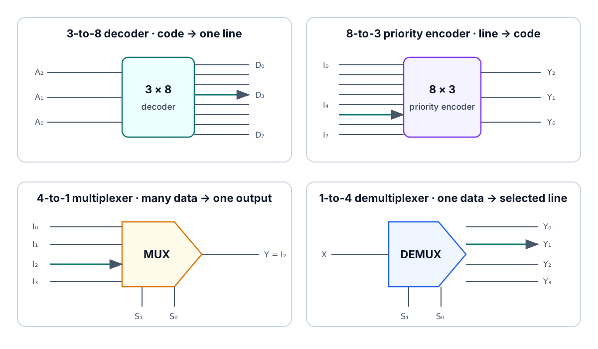
Decoder
An -to- decoder activates one output corresponding to an -bit input code. For a 2-to-4 active-high decoder with enable :
Decoders select memory words, registers, I/O interfaces, or one control line from an opcode. If an -bit code contains unused combinations, the corresponding decoder outputs are unused or assigned safe behavior.
Larger decoders can be expanded from smaller ones. A 3-to-8 decoder can be built with two enabled 2-to-4 decoders: the most-significant input enables one half while the other two inputs select within that half.
Encoder
An encoder produces a code identifying an asserted input. A simple -to- encoder assumes exactly one input is active. A priority encoder removes that assumption by choosing the highest-priority active input and usually producing a valid bit.
Multiplexer
A -to-1 multiplexer routes one of data inputs to one output using select inputs. For a 4-to-1 multiplexer:
Putting one multiplexer on every bit position creates a common bus selector. Four 4-bit registers require four 4-to-1 multiplexers—one per bus bit—not one multiplexer for the whole word.
Demultiplexer
A demultiplexer routes one data input to one selected output. With the input tied to 1, its behavior resembles a decoder. Demultiplexers distribute an enable pulse or serial data stream to a selected destination.
Registers
A register is a group of flip-flops sharing control signals. An -bit register stores an -bit word. Registers are faster and more directly connected to processor logic than main memory, so they hold operands and intermediate results.
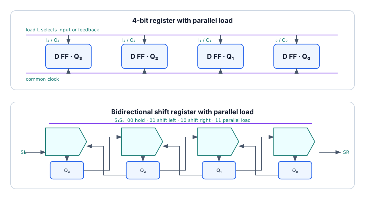
Basic register
Four D flip-flops with a common clock form a 4-bit register. If they also share an asynchronous clear, one clear signal forces every stored bit to zero. On the active clock edge,
Parallel load
Clock gating can prevent unwanted changes, but directly gating a clock creates skew and glitch risks. A safer design keeps the clock common and selects either the old value or new input:
When , the next edge loads ; when , feedback reloads , so the register holds.
Shift register
A shift register moves each stored bit to a neighboring stage on each active clock. For the ordering , the source note’s right-moving example uses
If and the current word , the next word is 1011; the old is shifted out. Always define bit ordering before calling a shift “left” or “right.”
Bidirectional shift register with parallel load
| Register operation | Typical input selected for stage | |
|---|---|---|
| 00 | Hold | |
| 01 | Shift left/down | Neighbor or serial boundary input |
| 10 | Shift right/up | Neighbor or serial boundary input |
| 11 | Parallel load |
This circuit is often called a universal shift register. A 4-to-1 multiplexer before each flip-flop selects one of the four next-state sources.
Shift types
- Logical shift: inserts zero; useful for unsigned scaling by powers of two.
- Arithmetic right shift: repeats the sign bit; preserves a two’s-complement sign.
- Circular shift/rotate: feeds the bit shifted out at one end back into the other.
Binary Counters
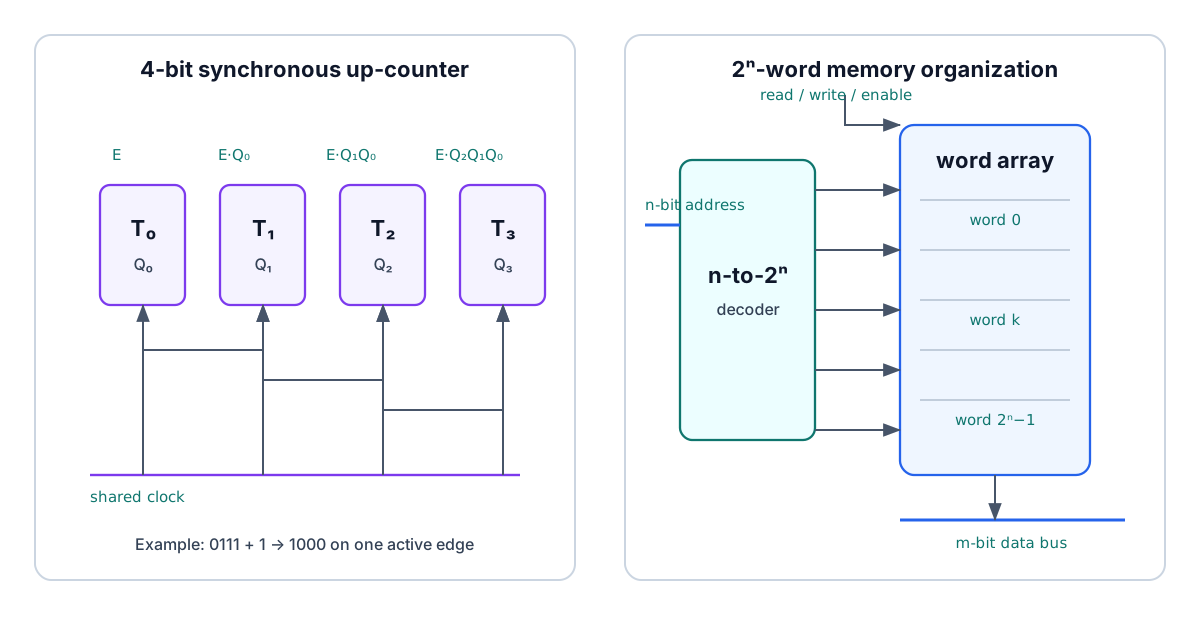
A binary counter is a register whose next state is the current binary value plus or minus one. In a synchronous up-counter with enable :
Each bit toggles only when every less-significant bit is 1. Starting from 0111, one enabled clock produces 1000; the three low bits clear while the high bit sets on the same edge.
A down-counter can track iterations in multiplication or division. A zero detector asserts when
Memory Unit as a Digital Component
A memory is specified as number of words × bits per word. A 1K × 8 memory stores words of 8 bits:
- address inputs: ;
- bidirectional data lines: 8;
- total stored bits: bits.
The address decoder activates one word line. A read exposes that word on the data bus; a write stores the data-bus value in the selected word when write enable is asserted.
| Capacity | Addressable locations | Address bits |
|---|---|---|
256 × 16 | 256 words | 8 |
1K × 8 | 1024 words | 10 |
64K × 32 | 65,536 words | 16 |
The number of data lines follows word width, not total capacity. Byte-addressable and word-addressable systems can therefore require different address widths for the same total number of stored bits.
Timing and Reliable State Changes
A logic diagram says which value should be produced; timing determines whether a clocked circuit can actually store that value correctly.
| Timing term | Meaning |
|---|---|
| Clock-to-Q delay | Time after an active edge before a source flip-flop’s output is valid. |
| Propagation delay | Worst-case time for a change to pass through combinational logic. |
| Setup time | Minimum time a destination input must be stable before its active edge. |
| Hold time | Minimum time the input must remain stable after the edge. |
| Clock skew | Difference between clock-arrival times at two storage elements. |
| Critical path | The longest register-to-register combinational path; it limits clock frequency. |
For a conservative single-cycle path,
If ps, the longest decoder/multiplexer path is ps, setup time is ps, and allowed skew is ps, then
Shortening a noncritical path does not raise ; the critical path must be reduced. Hold time is a separate minimum-delay requirement and cannot be repaired merely by choosing a slower clock.
An asynchronous input may change near a clock edge and leave a flip-flop temporarily metastable, neither a reliable zero nor one. A synchronizer—commonly two flip-flops in series—greatly reduces the probability that this uncertainty reaches the rest of a synchronous system. It does not make two unrelated clocks identical; multi-bit transfers still need a handshake or an asynchronous FIFO.
Worked Design: Four-Mode Register
Suppose , parallel input , serial-left input , and serial-right input .
| Control | Selected operation | Next |
|---|---|---|
| 00 | Hold | 1010 |
| 01 | Shift toward the most-significant end, insert at LSB | 0101 under the stated bit convention |
| 10 | Shift toward the least-significant end, insert at MSB | 0101 |
| 11 | Parallel load | 0111 |
The two shifts happen to produce the same word for these particular boundary bits and current pattern. That coincidence is not a circuit equivalence; change or and the results diverge.
Self-Check
- How many outputs and minterms does a 4-to-16 decoder generate?
- Why is a priority encoder necessary when multiple interrupt requests may be high?
- A
2K × 16memory contains how many bits and needs how many address lines? - What control selects parallel load in the universal-register table?
- A path has ps, ps, ps, and ps. What clock period and maximum frequency does it permit?
Answers
- Sixteen outputs/minterms.
- It defines which request wins and produces a deterministic code.
- bits and 11 address lines.
- .
- ps, so GHz.