Computer Organization
Distinguish architecture from organization, identify the functional units of a stored-program computer, and trace instructions through fetch, decode, and execution.
Updated
Learning objectives
- Distinguish computer architecture, organization, hardware, software, and firmware
- Explain the roles and connections of the processor, memory, and input-output units
- Trace a stored-program instruction through fetch, decode, execute, and write-back
- Separate data flow, address flow, and control flow
- Calculate CPU execution time from instruction count, CPI, and clock rate
Prerequisites
- Binary numbers and elementary digital logic
Computer architecture explains the contract visible to a programmer and the structures that make that contract run. The subject therefore connects two views:
```text program and data → instruction-set contract → processor organization → digital hardware ```
Central idea: architecture specifies what a machine does; organization explains how a particular machine does it.
Architecture, Organization, and Implementation
The terms are related but not interchangeable.
| Term | Meaning | Representative examples |
|---|---|---|
| Computer architecture | Attributes that directly affect the logical execution of programs | Instruction set, data widths, addressing modes, visible registers, I/O mechanisms |
| Computer organization | Operational units and interconnections that realize the architecture | Control signals, buses, cache structure, memory technology, pipeline depth |
| Hardware | Physical electronic and electromechanical components | Processor chip, RAM, disk, keyboard, wires |
| Software | Instructions and data manipulated by the machine | Operating system, compiler, application, input dataset |
| Firmware | Persistent programs stored in non-volatile electronic storage | Boot code, device-controller code, embedded-system control program |
Two processors may implement the same architecture while using different organizations. A program sees the same instructions, but one processor might use a five-stage pipeline and another a deeper pipeline with larger caches. Conversely, changing an instruction encoding changes the architecture because machine-code programs can observe it.
Firmware sits between ordinary software and hardware. It is program logic retained when power is removed and is normally changed less often than application software. Modern firmware can be updated, but its persistence and close relationship with a device distinguish it from ordinary programs.
Functional Units
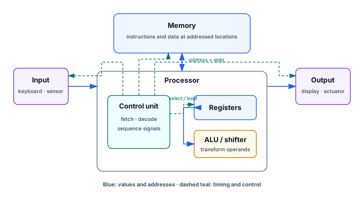
Input and output
Input units translate information from the external world into the binary representation used internally. Output units perform the reverse translation. Peripherals differ greatly in speed and representation, so an interface unit supplies data registers, status information, and timing control between a peripheral and the processor.
Memory
Memory stores both instructions and data. Each location has an address, and a read or write operation selects one location at a time. If a memory contains addressable locations, it needs address bits. A `64 KiB` byte-addressable memory therefore has locations and a 16-bit address.
Processor
The processor contains:
- a control unit, which fetches and decodes instructions and generates enabling signals;
- an arithmetic logic unit (ALU), which performs arithmetic, logical, and comparison operations;
- registers, which hold operands, addresses, instructions, status, and intermediate results close to the ALU.
The control unit is not normally the source of operand data. It selects routes and operations. The datapath—registers, buses, ALU, and shifter—carries and transforms the values.
Three Kinds of Information Flow
| Flow | Typical contents | Example |
|---|---|---|
| Data | Operand or instruction bits | Memory word transferred into the instruction register |
| Address | Identity of a memory or I/O location | Program counter copied to the memory address register |
| Control | Meaning and timing of a transfer | `MemoryRead`, `LoadIR`, `ALU=ADD`, `WriteR1` |
Treating every line as “data” hides the design problem. For a load instruction, an address must first become valid, a read command must be asserted, memory must return data, and only then may the destination register load.
The Stored-Program Operational Concept
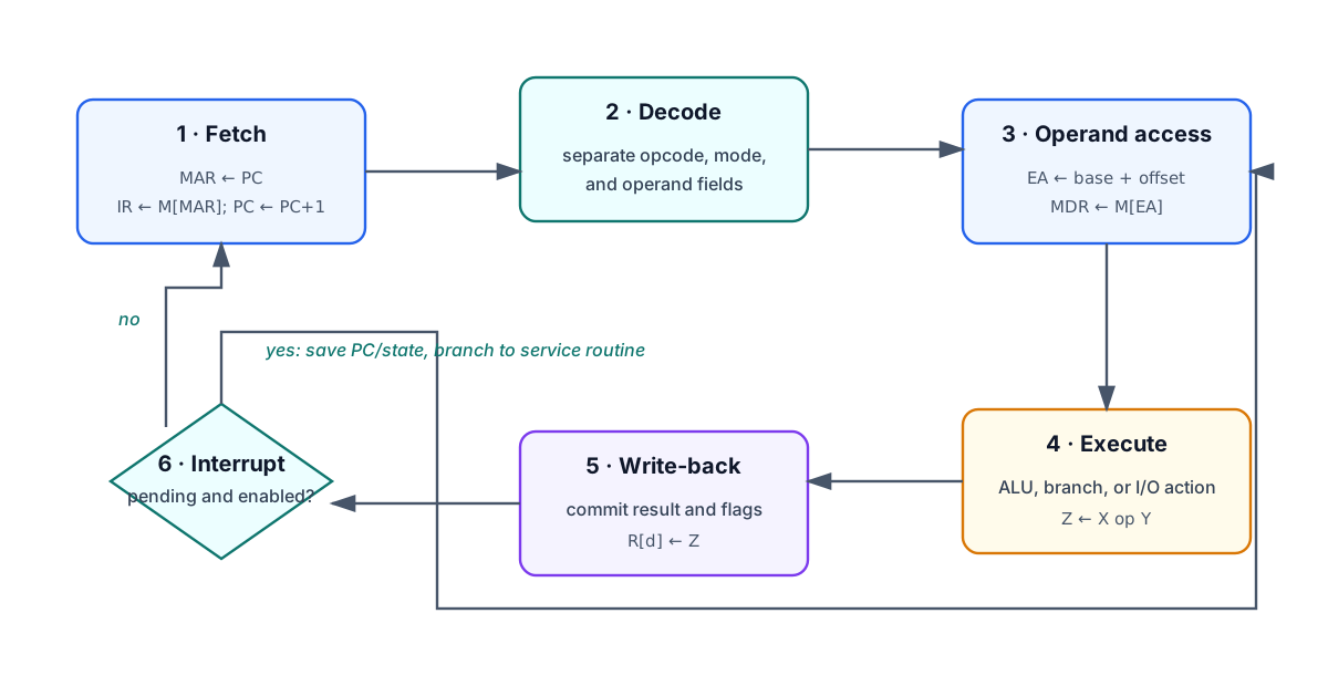
Instructions and ordinary data reside in memory as binary words. The program counter () identifies the next instruction. The instruction register () holds the current instruction while it is decoded and executed.
Fetch
A representative fetch uses temporary memory registers:
The transfers cannot all be assumed instantaneous. must hold a stable address while memory is read; captures the returned word; then preserves the instruction for decoding.
Decode and operand access
The opcode field selects the operation. Addressing-mode and operand fields identify registers, constants, or memory locations. An effective address may require an additional ALU calculation before the operand can be fetched.
Execute and write-back
For an arithmetic instruction, the control unit selects operands, chooses an ALU function, and enables the destination register. For an I/O instruction, it enables the appropriate interface. A branch may replace rather than writing an arithmetic result.
Interrupt check
After an instruction reaches a safe completion point, the processor may test pending enabled interrupts. If one is accepted, it saves enough state to resume later and transfers control to an interrupt-service routine.
A Complete Numeric Trace
Suppose memory contains:
| Address | Instruction or data |
|---|---|
| `0x020` | `LOAD R1, [0x180]` |
| `0x021` | `ADD R1, [0x181]` |
| `0x022` | `STORE R1, [0x182]` |
| `0x180` | `7` |
| `0x181` | `5` |
Initially . The visible effects are:
| Instruction | Operand activity | Result | Next |
|---|---|---|---|
| `LOAD` | Read | `0x021` | |
| `ADD` | Read ; ALU computes | `0x022` | |
| `STORE` | Send to memory | `0x023` |
The architecture describes these effects. The organization determines whether the operand comes through a shared bus, how many clock cycles each instruction needs, and whether the memory reference hits in a cache.
Measuring Execution Time
A useful first processor-performance equation is
If a program executes instructions at an average CPI of on a processor,
A higher clock rate alone does not guarantee a faster program: instruction count and CPI may change with the architecture, compiler, caches, and pipeline. Throughput—the amount of work completed per unit time—is also different from the latency of one task.
Comparing processors correctly
For one fixed workload, performance is the reciprocal of execution time. If machine A completes it in and machine B in , then
Suppose the same compiled program executes instructions on two processors:
| Processor | Clock rate | Average CPI | CPU time |
|---|---|---|---|
| A | GHz | s | |
| B | GHz | s |
Although B has the higher clock rate, A is times as fast for this program. A fair comparison must hold the workload constant and account for instruction count, CPI, and clock period together. Wall-clock time may additionally include operating-system delay and I/O; the CPU-time equation models time spent executing on the processor.
Abstraction Without Mystery
Each level depends on the one below it:
- Applications express algorithms.
- Compilers translate them into an instruction set.
- The processor organizes register transfers to implement each instruction.
- Digital circuits implement the registers, ALU, memory, and control.
An abstraction hides detail, but it does not remove causality. A cache miss, branch hazard, or slow I/O transfer becomes visible when lower-level timing changes program performance.
Design Checklist
When reading any architecture diagram, ask:
- Which elements store state?
- Which elements compute combinational results?
- Where do addresses travel?
- Where do operands and instructions travel?
- Which control signal makes each transfer permanent?
- On which clock edge does the new state become visible?
If those six questions have concrete answers, the diagram describes an executable machine rather than a collection of boxes.
Self-Check
- Classify “the instruction has a 12-bit address” and “the memory uses DRAM chips” as architecture or organization.
- How many address bits are required for a byte-addressable `4 MiB` memory?
- Why must the instruction register retain the fetched instruction after memory begins servicing another address?
- A program has instructions, CPI , and clock rate GHz. Find its CPU time.
- If one processor finishes a workload in 12 s and another in 8 s, what is the second processor’s speedup?
Answers
- The 12-bit instruction address is architectural; DRAM technology is organizational.
- bytes, so 22 address bits are required.
- Decode and execution still need stable instruction bits after the memory data path is reused.
- second.
- times.